engineering11 min read
The Architectural Logic of Logic Gates
Every digital marvel of the modern era, from the smartphone in a pocket to the sophisticated guidance systems of interplanetary probes, is built upon a singular, elegant foundation: the manipulation...
Every digital marvel of the modern era, from the smartphone in a pocket to the sophisticated guidance systems of interplanetary probes, is built upon a singular, elegant foundation: the manipulation of binary signals through logic gates. These physical manifestations of Boolean algebra serve as the fundamental building blocks of digital circuitry, acting as the decision-makers that process information in the form of electrical pulses. To understand the architectural logic of these gates is to understand the language of modern engineering itself, where complex computational problems are decomposed into a series of simple, deterministic switches. By abstracting away the messy reality of continuous voltage into discrete logical states, engineers can construct reliable systems that perform billions of operations per second with near-perfect accuracy.
This tabular representation allows for the rigorous analysis of complex systems before they are physically fabricated. In modern Electronic Design Automation (EDA) tools, truth tables are often abstracted into hardware description languages, but the underlying logic remains grounded in these binary relationships. Whether analyzing a single gate or a thousand-gate network, the truth table remains the "source of truth" for digital logic, ensuring that the architecture behaves exactly as intended under every conceivable state.
The Binary Foundation of Logic
The genesis of modern digital hardware lies in the transition from analog signal processing to discrete binary computation. In an analog system, information is represented by continuously varying voltages, which are inherently susceptible to noise, thermal fluctuations, and signal degradation over distance. Digital systems overcome these limitations by employing electronic switching, where transistors operate not as amplifiers, but as binary switches that are either fully "on" or fully "off." This binary paradigm simplifies the engineering challenge significantly; instead of measuring the exact value of a signal, the system only needs to determine whether a voltage level falls within a specific range to be categorized as a logical high or low. Quantifying these high and low voltage states is the primary task of the physical layer in digital logic circuits. In a typical Transistor-Transistor Logic (TTL) system, a logical high (1) is generally represented by a voltage between 2.0 and 5.0 volts, while a logical low (0) is represented by a voltage between 0.0 and 0.8 volts. The gap between these ranges, known as the noise margin, provides a critical buffer that prevents minor electrical interference from causing bit-flip errors. This robust categorization allows engineers to treat electrical signals as abstract mathematical variables, enabling the construction of digital logic circuits that maintain their integrity across millions of integrated components. The historical shift toward this binary foundation was catalyzed by Claude Shannon’s 1937 master’s thesis, where he demonstrated that the switching behavior of relay circuits could be described using the nineteenth-century algebraic system developed by George Boole. By mapping electrical pathways to Boolean expressions, Shannon provided the theoretical bridge that allowed engineers to design hardware using formal logic. Today, this principle is scaled to an unimaginable degree, with modern microprocessors containing billions of microscopic Complementary Metal-Oxide-Semiconductor (CMOS) transistors. Each of these transistors functions as a high-speed switch, collectively executing the Boolean operations that define the behavior of all software.Core Operations of AND OR NOT Gates
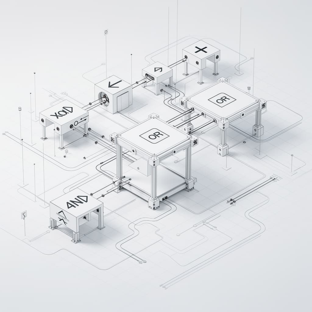
The vast complexity of digital architecture is constructed from a small set of primitive operations, most notably the AND OR NOT gates. The AND gate performs what is known in formal logic as conjunction; its output is high if and only if all of its inputs are simultaneously high. In a physical circuit, an AND gate acts as a series of switches where a break in any part of the chain results in a loss of signal at the terminus. This operation is essential for masking signals or ensuring that multiple conditions are met before a specific action—such as an arithmetic carry or a memory write—is executed by the processor. In contrast to the restrictive nature of conjunction, the OR gate facilitates inclusive disjunction, where the output is high if at least one of its inputs is high. If we imagine the AND gate as a series connection, the OR gate is best visualized as a parallel arrangement of switches where any single closed path completes the circuit. This gate is fundamental for combining signals from different sources, such as a computer receiving an interrupt signal from either a keyboard stroke or a mouse movement. Mathematically, the OR operation is often represented by the plus symbol in Boolean notation, such as $Y = A + B$, though it should not be confused with traditional decimal addition. The NOT gate, or inverter, represents the simplest yet most transformative of the primary gates because it operates on a single input to perform signal inversion. If the input is a logical high, the NOT gate outputs a logical low, and vice versa, essentially acting as a logical "mirror." Inversion is the cornerstone of signal timing and differential signaling, allowing engineers to create complementary states that are necessary for complex memory elements and clock cycles. Without the ability to flip a bit's state, a digital system would remain static, unable to perform the cyclical transitions required for state-driven computation.Analyzing Truth Tables for Logic Gates
To formalize the behavior of these electronic components, engineers utilize truth tables for logic gates, which provide an exhaustive mapping of every possible input combination to its corresponding output. A truth table serves as a deterministic contract; it guarantees that for a given set of binary inputs, the circuit will always produce the exact same result. For a two-input gate, the table consists of four rows representing the four possible permutations of $(0,0), (0,1), (1,0),$ and $(1,1)$. As the number of inputs $n$ increases, the complexity of the truth table grows at a rate of $2^n$, providing a comprehensive view of the gate's functional logic. The utility of truth tables extends beyond simple documentation; they are the primary tool for evaluating sequential input permutations and verifying circuit designs. By laying out the logic in a tabular format, an engineer can quickly identify redundant logic or unexpected edge cases where an output might trigger prematurely. For example, the truth table for an XOR (Exclusive OR) gate reveals a unique pattern where the output is high only when the inputs differ, a property that is indispensable for binary addition and parity checking. These tables essentially translate the abstract "ideas" of logic into a concrete data structure that can be used for simulation and automated testing. Consider the truth table for a standard 3-input AND gate, which illustrates the deterministic nature of conjunction:| Input A | Input B | Input C | Output Y |
|---|---|---|---|
| 0 | 0 | 0 | 0 |
| 0 | 0 | 1 | 0 |
| 0 | 1 | 0 | 0 |
| 0 | 1 | 1 | 0 |
| 1 | 0 | 0 | 0 |
| 1 | 0 | 1 | 0 |
| 1 | 1 | 0 | 0 |
| 1 | 1 | 1 | 1 |
Universal Gates and System Efficiency
While AND, OR, and NOT gates form the conceptual core of digital logic, practical engineering often favors the use of "universal gates"—specifically the NAND and NOR gates. A gate is considered universal if any other Boolean function can be implemented using only that type of gate. For example, a NOT gate can be created by tying both inputs of a NAND gate together, and an AND gate can be formed by following a NAND gate with an inverter. This property of functional completeness allows manufacturers to streamline production by creating vast arrays of identical NAND gates, which are then interconnected to form the specific logic required by the system. Constructing logic with NAND and NOR gates is not just a matter of convenience; it is a fundamental strategy for increasing system efficiency and reducing fabrication costs. In CMOS technology, a NAND gate is physically smaller and faster than an AND gate because the AND operation actually requires two stages—a NAND followed by an inverter—whereas NAND is implemented in a single stage. Consequently, a circuit built primarily from NAND gates will generally consume less power and have a shorter propagation delay than one built from separate AND and NOT gates. This efficiency is the reason why NAND flash memory and many microcontrollers are designed around these universal primitives. The historical significance of universal gates is perhaps best exemplified by the Apollo Guidance Computer (AGC), which was the first significant system to utilize integrated circuits. To simplify the manufacturing process and increase reliability in the harsh environment of space, the AGC was built using approximately 2,800 identical 3-input NOR gates. Every logic function in the computer, from basic math to flight control, was synthesized from these NOR gates. This architectural choice proved that functional completeness is not merely a mathematical curiosity but a robust engineering philosophy that can power humanity’s most ambitious endeavors.Decoding Standard Logic Gate Symbols
In the realm of engineering schematics, logic gate symbols act as a standardized visual language that allows designers to communicate complex logical flows at a glance. There are two primary standards for these symbols: the distinctive shape notation (ANSI/IEEE Std 91-1984) and the rectangular notation (IEC 60617-12). The distinctive shape notation is more widely used in North America and by students, featuring a flat-back D-shape for AND, a curved-back pointed shape for OR, and a triangle with a small circle for NOT. These shapes are designed to be recognizable even when drawn by hand, facilitating rapid prototyping and debugging of circuit diagrams. Reading high-level logic schematic flows requires an understanding of the small but crucial details within these symbols, such as the "bubble" or "inversion circle." A circle placed at an input or output pin indicates a logical negation, turning an AND gate into a NAND gate or an OR gate into a NOR gate. This visual shorthand is vital because it signifies "active-low" logic, where a signal performs its intended function when at a low voltage state rather than a high one. Engineers must be adept at tracing these signals through multiple stages, ensuring that the polarity of the logic remains consistent throughout the entire signal path."The small circle, or 'bubble,' on a logic gate symbol is perhaps the most significant single mark in a digital schematic, as it defines the transition between high-assertive and low-assertive logic states."Beyond the basic gates, symbols also exist for complex modules such as buffers, which do not change the logic state but strengthen the signal to drive more inputs (a concept known as "fan-out"). In advanced schematics, these symbols are integrated into bus lines and multiplexer blocks, creating a hierarchy of information flow. By mastering these graphic representations, an engineer can "read" a circuit board like a map, identifying the logical bottlenecks and critical paths that determine the overall performance of the digital hardware.
Mathematical Boolean Logic in Engineering
The design and optimization of logic gates are governed by the rigorous laws of Boolean algebra, which allow engineers to manipulate logical expressions with the same precision as traditional arithmetic. The laws of commutation and association, for instance, dictate that the order of inputs does not affect the output of an AND or OR operation, while the distributive law allows for the expansion and factoring of logic terms. One of the most powerful tools in this mathematical arsenal is De Morgan's Laws, which provide a bridge between AND and OR operations: $\overline{A \cdot B} = \overline{A} + \overline{B}$ and $\overline{A + B} = \overline{A} \cdot \overline{B}$. These laws allow designers to swap gate types to match available hardware without changing the underlying logic. To handle the complexity of larger expressions, engineers employ visual minimization techniques such as Karnaugh Maps, or K-maps. A K-map is a grid-based representation of a truth table where cells are arranged in Gray code order, meaning only one bit changes between adjacent cells. This arrangement allows for the visual identification of patterns and the grouping of common terms, which can then be simplified into a "Minimal Sum of Products" (SOP) expression. By minimizing the Boolean expression, the engineer reduces the total number of physical gates required, which directly translates to lower heat dissipation, reduced silicon area, and increased operational frequency. Boolean logic in engineering also involves the management of "don't care" conditions, where certain input combinations are guaranteed never to occur or where their output does not affect the system's performance. In a K-map, these conditions can be treated as either 0 or 1 to achieve the greatest possible simplification. This level of mathematical optimization is what allows modern chips to pack billions of functions into a few square millimeters of silicon. Without these formal laws, digital design would be a chaotic process of trial and error rather than a predictable science of logical refinement.Complexity in Integrated Digital Logic Circuits
As individual logic gates are combined, they evolve from simple decision-makers into complex digital logic circuits capable of performing high-level computation. These circuits are generally categorized into two types: combinational and sequential. Combinational logic, such as an adder or a multiplexer, produces an output based solely on the current state of its inputs. For example, a Half-Adder uses an XOR gate to calculate the sum of two bits and an AND gate to determine the carry bit. These units are the "muscles" of the CPU, executing the arithmetic and logical instructions defined by the software. However, computation requires more than just immediate calculation; it requires the ability to remember past states, which is where sequential logic enters the architecture. By introducing feedback loops, where the output of a gate is fed back into one of its inputs, engineers can create bistable elements known as latches and flip-flops. These components serve as the basic units of memory storage, holding a single bit of information until it is explicitly changed by a clock signal. The transition from pure logic to memory is what allows a processor to follow a sequence of instructions, maintaining its state through billions of cycles. The ultimate realization of this logic is the Arithmetic Logic Unit (ALU) and the Control Unit of a modern microprocessor. These massive networks of gates are orchestrated by a global clock, ensuring that signals propagate through the various stages of the logic paths in perfect synchronization. From a single NOT gate to a 64-bit multi-core processor, the architectural logic remains remarkably consistent: it is a hierarchy of switches, defined by truth tables, optimized by Boolean algebra, and realized in the physical movement of electrons. This seamless transition from abstract math to physical reality is the defining achievement of digital engineering.References
- Mano, M. M., and Ciletti, M. D., "Digital Design: With an Introduction to the Verilog HDL, VHDL, and SystemVerilog", Pearson, 2017.
- Shannon, C. E., "A Symbolic Analysis of Relay and Switching Circuits", Transactions of the American Institute of Electrical Engineers, 1938.
- Floyd, T. L., "Digital Fundamentals", Pearson Education, 2015.
- Wakerly, J. F., "Digital Design: Principles and Practices", Prentice Hall, 2005.
Recommended Readings
- Code: The Hidden Language of Computer Hardware and Software by Charles Petzold — A brilliant narrative that builds a computer from scratch using nothing but flashlights and basic logic, perfect for building deep intuition.
- The Art of Electronics by Horowitz and Hill — The definitive reference for practical circuit design, offering extensive insights into the physical implementation of logic gates.
- Computer Architecture: A Quantitative Approach by Hennessy and Patterson — This text explores how basic logic gates are organized into the high-performance architectures that define modern computing.
logic gatestruth tables for logic gatesAND OR NOT gatesdigital logic circuitslogic gate symbolsboolean logic in engineering